
The new PCBs (I always buy two in case there is a problem with one) arrived earlier this week and I am currently awaiting the delivery of all the components. Once they arrive I can hopefully get this PCB up and running as soon as possible.
Below are the major differences between this version compared with the previous iterations with a little bit more of an explanation than was given in the Kickstarter update.
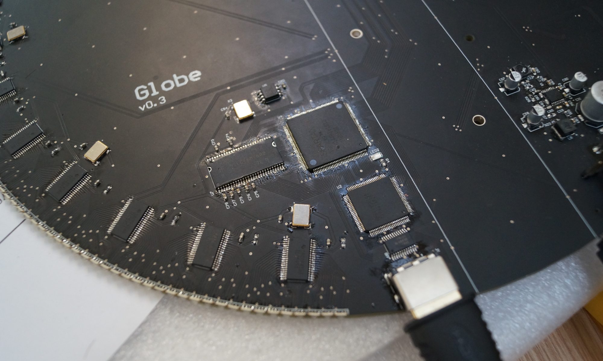
- Full integration of a Raspberry Pi Compute Module – PCB version 0.3 had HDMI and USB data transmitted via the slip rings, with TFP401 and FTDI 2232 interface chips. In reality it makes a lot more sense to have the HDMI and USB source on the PCB itself (reducing slipring cost, increasing lifetime and generally making things a lot more simple overall). Though v0.3 did have the capability of hosting a Raspberry Pi Zero W, this version of the Pi wasn’t really very well suited due to its HDMI and USB connections being board to wire. It’s virtually impossible to get hold of large quantities of the Zero anyway since most retailers limit it to 1 per customer.
The Raspberry Pi compute is the version that is designed to be embedded into commercial designs and can be appropriated in large quantities. It comes in a 200 pin SODIMM compatible package and breaks out basically all connectivity options, meaning I can have the HDMI signals go straight out onto my own PCB which is perfect. - Addition of an ESP8266 for Wifi connectivity. One of the downsides of the Pi Compute is it is pretty much as bare bones as possible, no inbuilt wifi antenna etc. Therefore we need to stick one of our own on there. One option was to put just a chip on there and then create a trace antenna, but when you compare the cost and complexity of that with buying a premade and test solution like the ESP8266 there really is not contest.
- Addition of an HM11-Ble for Bluetooth. The Bluetooth module is mostly there to test, in case I want to use one in the final design. The reason I want Bluetooth is because I may want a way to communicate between the main PCB (which you will be able to communicate with), and the motor controller i.e. to turn the damn thing off remotely. I will be seeking feedback prior to making a final decision on this – it isn’t a huge additional expense to put an extra couple of bluetooth modules in per unit, but then again, how often are you really going to want to turn the display off without simply going and doing it manually. I could potentially put wifi on the motor controller, but then that poses potential security/larger connectivity issues.
- Removal of the FTDI 2232 module – the FPGA will now be programmed directly by the Pi via JTAG using OpenOCD. This should work…theoretically. I’ve been through the documentation, it says it can be done, I’m really hoping it can because it does make life a lot easier. Goodbye FTDI interface chip and all the associated components that go with it, hello simply hooking up the right JTAG lines from the Pi to the FPGA. If this doesn’t work then the solution is to put the FTDI chip back on, and instead pull the USB lines out of the Pi, but I am fairly optimistic.
- Modification of the voltage regulator to allow the additional 1.8V supply needed for the Pi, minimise cost and BOM lines. The old voltage regulator took 5V in, and provided a 3.3 and 1.2V output that served pretty much everything on the PCB. It was also unnecessarily complex, having about 20 different resistors with bizarre values like 40.2K to provide all the necessary dividers and so on for the feedback voltages etc. The new supply is far more simple. I have a single, fixed value 3.3V regulator (providing up to 3A) which most components require, and a dual 1.8/1.2V regulator providing 600mA on either channel, required for the FPGA and Pi. This setup has significantly reduced my BOM lines, and cost in general, so I’m pretty pleased with it, not that TI’s power architect wanted to make things easy.
- Addition of 48 LEDs, bringing the total resolution now to 1920×288. Globe was advertised with a resolution of 1920×256, but in reality I wanted to push it a little bit higher than that, and 256 didn’t fit very nicely with the groups of 3 daisychained drivers (128 does not divide by 24 nicely), and so instead I switched up to 288. The FPGA will no longer receive a resolution of 1920×1080 from the Pi, which it used to divide down to 1920×270 (and drop 30 pixels where the shaft is). Instead it will receive a 1920×960 which it will drop down to 320 (and drop 32 pixels).
- Addition of a hall effect sensor so the image out data is now controlled based on the rotation speed, not the image in speed (no more interlacing issues). I don’t think I ever did fully explain the interlacing issue of the last display here so here it goes… It is quite a difficult thing to try and describe but essentially the “left” side of the display is displaying data of half an image and 1 line offset from the “right” side of the display (left and right as if the PCB was flat facing the viewer). The theory being that in half a rotation period, the left side is exactly at the position that the right side was half an image ago. However, if the rotation speed isn’t exactly in sync with the frame rate (because we were controlling our image synchronisation with that, rather than the actual rotation speed) then that is not the case. Instead our left side is now a couple of horizontal pixels behind or ahead of where it should have been, and so you end up with every other line being slightly out of alignment. There was also the issue of the VSYNC pulse which, if you are using the HSYNC rising edge to decide when to shift a new line of data to the drivers, also threw everything out of sync (even if you made your vsync pulse as short as possible.
The long and short of it is, this next version should get rid of the old problem that you can see in the video and then all my media will look loads better, and a hall effect sensor is the best way to do that. - Removal of the HDMI interface chip, now the HDMI signals go directly to the FPGA and are decoded on chip. V0.4 was going to be an interim design, mostly to get the prototype back on its feet after the sliprings stopped reliably carrying HDMI signals (can’t blame them to be fair). While the HDMI connection required a wire, the DPI (display parallel interface) did not, and could be pulled off the GPIO pins. At the time, I was still trying to decide whether I was going to continue using the HDMI protocol (which would require either an expensive interface chip or decoding on the FPGA) or switch to DPI which I already essentially had the code implemented for and so making this switch, even if temporarily, didn’t seem like a terrible idea. However, as I waited for funds to be deposited, I started having a look at the possibility of implementing an interface on the FPGA, and it turned out it would indeed be possible, therefore lessening the requirement to have an interim DPI prototype.
- Adding additional mounting holes to allow compatibility with both the old shaft as well as with the next, much shorter, shaft. The old shaft was a ludicrous 70cm long monstrosity, which cost loads of money to make and was fairly unnecessary since it ran pretty much up the length of the board. Theoretically we shouldn’t need the new one to do so and we should be ok with it connecting up about 10cm of the PCB. I added some extra holes to allow us to do this securely, so that this PCB can be used with the old mechanical housing for rapid testing, and the new mechanical housing to test that too.
- Adding a molex edgemate at the bottom centre of the PCB, meaning the power connector is now embedded in the shaft, rather than coming out and connecting at the side. Because the next design uses a hall effect sensor (on the PCB) and a magnet (on the base next to the shaft) to measure the rotation speed, I can no longer have wires coming out of the shaft and connecting at the side (wires rapidly running over magnets = bad). It also wasn’t very elegant having a big old power connector there. The new design uses a molex edgemate connector which will actually sit nestled in the shaft and plug directly into the board which is pretty cool.
As a note to Molex – please create libraries for all your components. While Altium has an edge connector design wizard, this wizard completely omits things like PCB which you then have to add manually (which takes bloody ages to calculate and create). - Switching to a 1.6mm PCB down from 3.2mm. The edgemate connector requires a thickness of 1.6mm, and the 3.2mm was only used in the first place to be certain that the PCB wouldn’t disintegrate itself when spinning. Now that I know that this is fairly unlikely I am confident in switching back to the now required 1.6mm. I was pretty lucky that I found a fabrication house that even did 3.2mm PCB at a reasonable cost in the first place, and now that I will be back to a standard size I will be able to shop around for competitive quotes.
I haven’t got my good camera on me at the moment, I will pick it up on Thursday and get some much better shots, but here is the lovely new PCB ready to be soldered.
