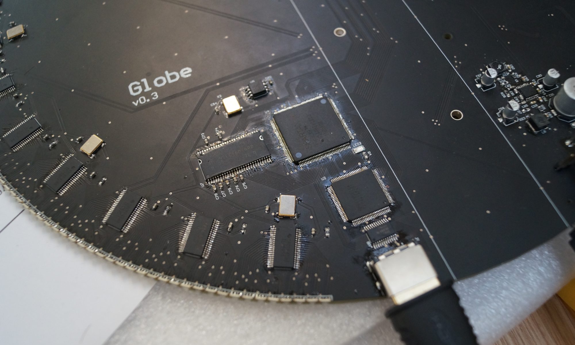

Ok so this one was mostly my fault. Despite all the time I spent agonising over the schematic entry I ended up cocking a few things up. I was considering pasting and hot airing the board rather than manually soldering but since this would require doing each side of the board all in one go and anticipating potential screw ups I decided to manually solder stage by stage, testing as I went…wise choice.
Before I detail all of these I will mention what went right:
- Voltage regulator: The voltage regulator does its job giving a nice clean 3.3V and 1.2V
- FTDI: The FT2232 does its job allowing me to program the FPGA and communicate with it.
- HDMI buffer: Does its job, level shifts nicely, impossible to tell if it does anything to the HDMI signal since A. the HDMI sockets screwed (more on that in a sec) and B. I don’t have easy access to a scope to check the signal anyway.
- FPGA: After some tinkering I was able to program the FPGA and test that it does at least something that I told it to.
So what went wrong?
- FPGA flash: I switched the SI & SO lines resulting in the flash being unprogrammable it first. Straightforward fix to cut the traces and swap the lines. After that it was programming happily.
- FPGA configuration: Some pins that should have been pulled high or low for configuration were not/connected to things which would pulling in the wrong direction. Fixed by cutting traces, rewiring and adding pull up/down resistors where needed.
- Thermal reliefs: The thermal relief connects for the polygons were too big (I failed to take into account the use of 2oz copper), making soldering the ground connection on pretty much all the components a massive pain. This caused occasional dry joints and in general slowed down the assembly.
- Untented vias under components: Putting vias under components was fairly mandatory for a 2 layer board with fairly dense component placement, leaving them untented was not. By not doing so caused the excess solder added during the SMD soldering process to cause a short behind the package legs between 3.3 and 1.2V. A simple continuity test between all power rails after this prevented any damage to the board but did require further time to be wasted visually inspecting and fixing any time such a problem did crop up.
- HDMI socket: Somehow during the move from Eagle to Altium the schematic component library got screwed with the negative and shield pins getting switched on every single data and clock line. To fix this should have been possible…just, but would have required some pretty ninja like cutting and wiring. Even then it may not have worked since the traces would no longer be matched lengths.
Aside from a few other trivial issues there wasn’t too much else that went wrong. Once I hit the HDMI issue and realised what a pain it would be to fix I decided that simply getting a new board made with all the other problems fixed would be the sensible route. While being another £250 expense which I could have really done without, I felt it would be best to have a prototype that didn’t have cut traces and wires hanging off it for any pictures that would feature in the Kickstarter campaign. It also gave me an opportunity to remove the clock and data buffers (unnecessary as I will send this data through the GS lines) and the ESP8266 wireless module (unnecessary due to the recently released Pi Zero having in built wifi).
So at the time of writing this my new PCB has just shipped from China – cue import duty, which should turn up towards the end of this week. The only manufacturing difference between this board and the last is the decision to go for a matte black solder mask, mostly just out of curiosity. I will have a little vote on which people would prefer.