
Before investing too much time and money in designing the full Globe PCB a smaller test board was needed. The purpose of this PCB was to test the following:
- TFP401 interface with FPGA
- SDRAM interface with FPGA
- Modifying EDIDs
- FPGA SPI controller & interface with TLC5951
- First version of code
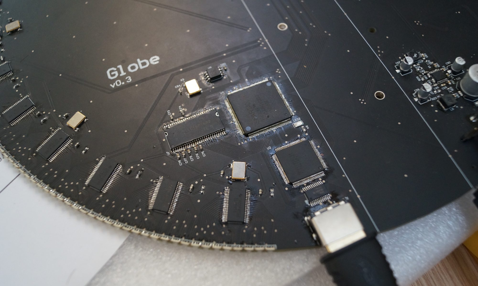
The board was designed as a shield for the Papilio Pro. The P. Pro is a development board with a Spartan 6 LX9, 64Mb of SDRAM and an FT2232 USB interface with 48 female headers. If you are interested in playing round with an FPGA it makes a great place to start.
The shield had a TFP401A, a couple of linear voltage regulators, 4 daisy-chained TLC5951s, an HDMI socket and a small EEPROM to hold the EDID.
at this point I hadn’t settled on the number of TLC5951 to be connected in series or the use of the HDMI buffer to handle the I2C level shifting for the EDID FPGA interface.
The nice thing about the code written for this test board was that it was more or less the code required for Globe. While it only made use of two of its SPI lines the code for all additional ones was implemented as well, all data that would be required for the full board was buffered, written to and read from the SDRAM.
The nice thing about the SPI control of the LED drivers is that it is pretty easy to tell whether the code is doing what it’s meant to be doing at a glance. If I make the PCB “screen” fully green, if the code is working then all the LEDs will become statically green. If the latch signal occurs incorrectly or the data ends up skewed during its buffering, even if a single bit is lost or appended to the data the resultant LED colour just becomes an ever changing jumble.
Suffice it to say, everything worked…eventually.
