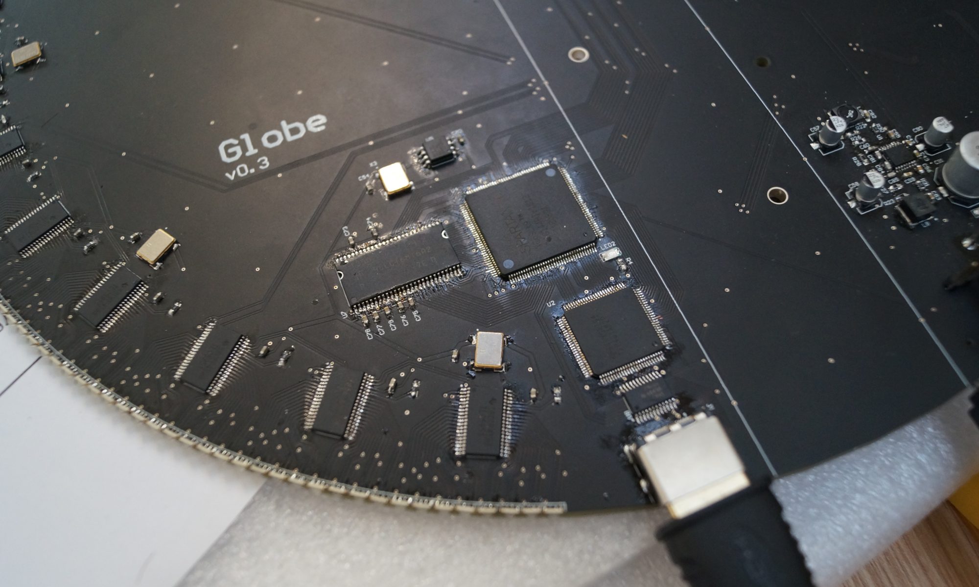
POV MKI used 4 PIC32s each controlling 4 TLC5951 LED drivers which each in turn drive 8 RGB LEDs, with one of the PICs acting as master and the other three as slaves. Since we are only increasing the number of LEDs, LED drivers and required SPI control lines, we can either apply more microcontrollers to the problem or switch over to using an FPGA. To use more microcontrollers would simply be too cumbersome (and a pain in the arse to try and interface video with) whereas an FPGA while being slightly more complex to code would make life far more simple in terms of overall circuit design and performance.
The Spartan 6 LX9 is the FPGA of choice, basically as beefy a chip as you are going to get while still coming in an easy to solder TQFP package. Due to having LEDs on both the left and right side of the PCB, the image data for LEDs on one side of the board needs to be offset by half an image from the other side. This means one of two things needs to be done, either the data being streamed via HDMI needs to fudged so that every second horizontal line is half an image offset or the whole image needs to be buffered on the PCB side and appropriately accessed by the FPGA.
- To do the former would be an absolute nightmare either requiring everything that one wants to display to go through a program that does the fudging or rewriting the entire video driver
- To do the latter requires the use of an external memory module for the FPGA, one image requiring 1.382Mb (1920*240*24) and the LX9 only having 576Kb. In reality at least two images need to be stored, one for writing in and one for reading out.
The other matter that needs to be considered is the necessary data rate. If we are aiming for 15 FPS then our required data rate will be about 332Mb/s (1920*240*24*2) or just over 41MB/s. Luckily the SDRAM controller that Mike Field wrote can handle that (as long as reads and writes are performed at least semi-sequentially). The SDRAM module used is a 256Mb Micron MT48LC16M16, slightly overkill but it’s hard to get hold of anything smaller.
A TFP401 is used to decode the HDMI LVDS signals into nice 24bit output data with HSYNC, VSYNC, DE and Pixel Clock brought out for easy interfacing. Throw in a TPD12S016 HDMI buffer with inbuilt logic level shifter allowing the EDID to be handled by the FPGA, avoiding having to have an additional EEPROM to store it.
We will be sticking with the TLC5951 which I used in POV MKI. I really like this chip; it offers 12bit PWM control over each channel, a 30Mb/s data throughput, daisy chaining, up to 40mA per channel current sink and a host of features such as global brightness control for each channel. While it’s a bit irritating having to pad and transfer an additional 50% of data, since our images and HDMI data is only 24bit, the high data rate makes up for it. It also comes in both a DSO and a tiny VQFN (which will come in useful if the flex PCB design is explored).
Mark II will use 240 LEDs requiring 30 TLC5951 drivers. The maximum SPI transfer rate for the drivers is 30Mb/s, we can therefor calculate the maximum number of SPI drivers that can be run in with the calculation:
N = 30,000,000/(12*24*15*1920)
So N = 3.62, rounded down to 3, which conveniently results in 10 series of 3, easy to program, layout and route.
Power wise, three voltage supplies are needed: 5, 3.3 and 1.2 volts. The LEDs will require the highest current by far; if each LED channel requires 20mA that’s 60mA per LED*240 LEDs, coming out at 14.4A. For simplicity the board will be supplied by a single 5V supply rail with a current limit of 30A (always better to have a bit of headroom and most power supplies tend run most efficiently at ~50% load) which will use a dual output buck converter to provide the 3.3V and 1.2V. All the LEDs anodes can be connected to the 5V rail; the drivers providing the necessary current limiting. The total 3.3V current requirement should no more than 2A. The TPS54292 provides a 1.5 and 2.5A configurable voltage outputs which should be ample for this design. TIs’ Switcher Pro (soon to be replaced) makes designing your voltage regulator a lot easier than trying to work through equations from the data sheet, thumbs up to TI for that.
While the slip rings should be capable of transferring HDMI signals there is the possibility that they aren’t which is why I am including a Raspberry Pi Zero on the PCB. The Pi Zero is a pretty neat little bit of kit, much smaller and lighter than a regular Pi with minimal connectors on (2 micro USBs, 1 mini HDMI, SD card and 40 PIN GPIO header). In the worst case scenario I can connect the Pi Zero via a miniHDMI to HDMI cable to the port on the bottom of the board (yeah it will look pretty sketchy). For MKIII all the data connections via slip rings will be removed (unless there is an overwhelming demand for them) and instead a Pi Compute module will be added to allow Globe to appear as a networked computer enabling users to wirelessly control, stream content and even RDP to.